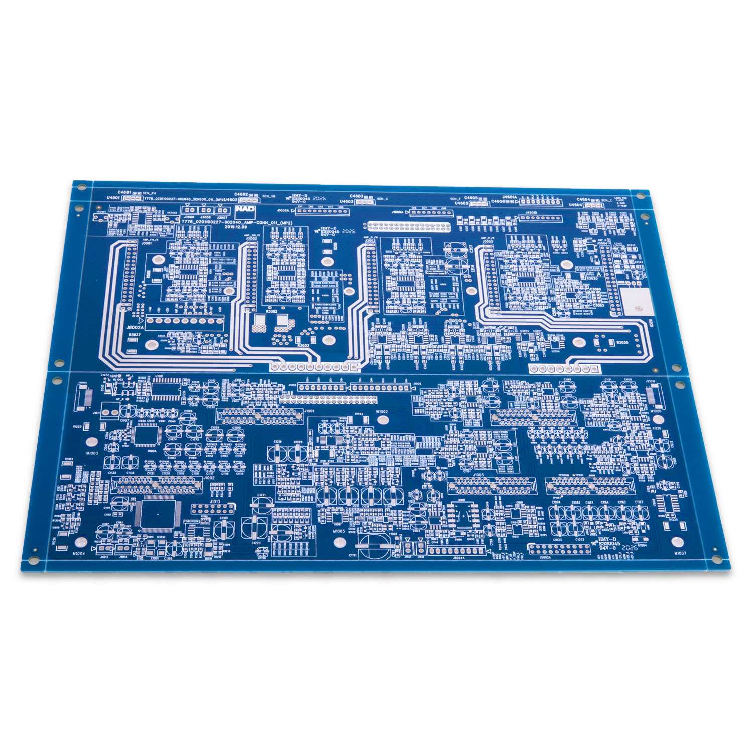
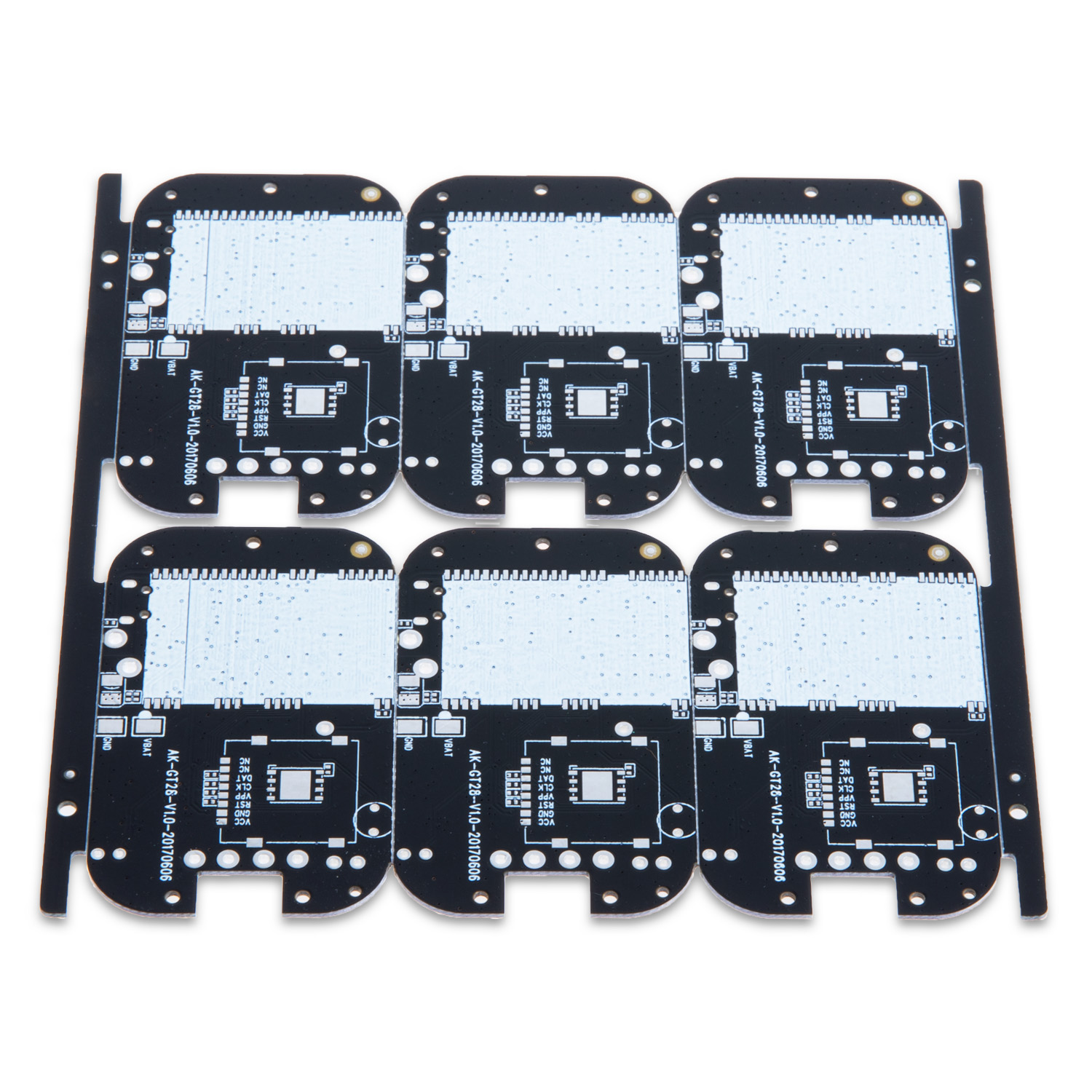
Manufacturing high-quality prototype multilayer PCBs (Printed Circuit Boards) is an essential step in the development of modern electronic devices. These boards are integral to complex electronics like smartphones, medical devices, and automotive systems. Whether you're designing a cutting-edge gadget or a new wearable device, understanding the manufacturing process for prototype multilayer PCBs is crucial for success.
At Hongmy, a trusted PCB manufacturer based in China, we specialize in creating prototype multilayer PCBs that meet the highest industry standards. In this article, we'll guide you through the key aspects of manufacturing high-quality prototype multilayer PCBs and the advantages of working with a reliable manufacturer like Hongmy.

What Are Prototype Multilayer PCBs?
A prototype multilayer PCB consists of multiple layers of conductive material, each separated by an insulating layer. These layers are laminated together to create a compact, high-performance circuit board. Multilayer PCBs are designed to provide higher circuit density and enhanced electrical performance compared to traditional single-layer or double-layer PCBs. They're commonly used in applications that require sophisticated functionality, such as smartphones, high-speed communication devices, and medical equipment.
Key Steps in Manufacturing Prototype Multilayer PCBs
1.Design and Schematic Layout
The first step in manufacturing a prototype multilayer PCB is creating a design layout. A designer uses specialized software to develop the schematic and ensure the proper routing of signals and power across the various layers. The key here is precision and attention to detail. Any mistakes in this stage can cause the entire project to fail.
At Hongmy, our team of expert engineers works with clients to finalize the design, making sure that the multilayer PCB layout is optimized for functionality and manufacturability.
2.Material Selection
The choice of materials for multilayer PCBs plays a vital role in the board's performance and longevity. The base material used for the layers can affect signal integrity, heat dissipation, and overall reliability. Common materials include FR4 (Fiberglass Reinforced Epoxy), high-frequency materials, and metal-core substrates. Hongmy uses only the best-quality materials to ensure durability and maximum performance.
3.Layer Alignment and Lamination
Once the materials are selected, the layers are carefully aligned, ensuring that all the layers fit precisely. The layers are then laminated together under high pressure and temperature to form a solid, multi-layered structure. This lamination process ensures that all components are securely bonded, and the board can handle the electrical loads it will experience during use.
4.Drilling and Via Formation
After the lamination process, holes are drilled to allow for the connection of electrical components across the various layers. This includes vias—small holes filled with conductive material that create electrical connections between the layers. At Hongmy, we use advanced drilling techniques and equipment to ensure precise via placement, which is critical for maintaining signal integrity and electrical performance.
5.Copper Plating and Etching
The next step is plating the drilled holes with copper to create the electrical connections. The copper is then etched to form the conductive tracks on the PCB. This process requires precision to ensure that the copper tracks align properly with the design and provide the necessary conductivity for the circuit.
6.Testing and Quality Control
Once the multilayer PCB is assembled, it goes through a rigorous testing process to ensure that it meets the required specifications. This includes both visual inspections and electrical tests to detect any potential issues such as shorts, open circuits, or improper component placements. Hongmy guarantees high-quality production through strict adherence to testing and quality control measures, ensuring that your prototype multilayer PCBs are free from defects.
7.Component Placement and Soldering
After the PCB passes testing, the components such as resistors, capacitors, and microchips are placed on the PCB. This is done using automated machines to ensure accuracy and efficiency. The components are then soldered onto the PCB using either wave soldering or surface mount technology (SMT). At Hongmy, we ensure that each component is placed correctly and securely to avoid any malfunction in the final product.

Advantages of Working with a Reliable Manufacturer like Hongmy
When it comes to manufacturing prototype multilayer PCBs, working with an experienced and reliable manufacturer like Hongmy can bring significant advantages:
Expert Engineering Team: Our engineers work with you to ensure your design is optimized for manufacturability and performance.
High-Quality Materials: We use the best materials to manufacture durable, high-performance PCBs that last.
Advanced Technology: We utilize state-of-the-art equipment to ensure precise drilling, copper plating, and etching for flawless results.
Quality Control: Rigorous testing and quality checks guarantee that your prototype multilayer PCBs meet the highest standards.
Fast Turnaround Time: We understand the importance of time in product development and offer fast, efficient prototyping services.
Conclusion
The process of manufacturing high-quality prototype multilayer PCBs involves careful design, material selection, and precise execution. By choosing a trusted manufacturer like Hongmy, you can ensure your PCBs meet the demands of your high-performance application. Whether you're creating the next smartphone, medical device, or innovative electronics, Hongmy provides the expertise and technology to bring your vision to life.
If you're ready to get started with your multilayer PCB prototype, contact Hongmy today. Our team is here to help you create the perfect circuit board for your needs!

